-
- Contact Us
- Privacy Policy
- term and condition
- Cookies policy

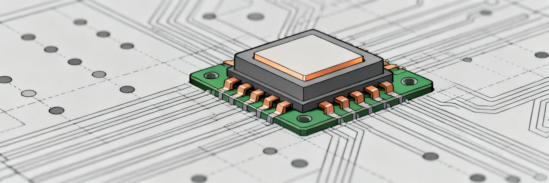
BAS16L Datasheet: Specs, Ratings & PCB Footprint Insights
The BAS16L datasheet consolidates the small-signal diode family’s declared ranges and measured behavior across multiple vendors to help hardware and PCB designers. Typical published ranges include reverse voltage around 75–100 V, continuous forward current near 200–215 mA, and surge capability up to ~4 A; common package footprints are DFN1006-2 / SOD882 (~1.0 × 0.6 mm). This article targets hardware/PCB designers and test engineers seeking clear specs, recommended land patterns, thermal guidance, and a practical design checklist.
Background: What “BAS16L” refers to (part family & common packages)
Point: BAS16L denotes a family of small-signal, fast-switching silicon diodes intended for compact board uses.
Evidence: Vendor datasheets consistently position these parts for signal steering, protection and high-voltage switching in constrained footprints.
Explanation: Designers pick BAS16L when they need high reverse voltage in a micro-package for clamping, steering or low-current switching where board area and parasitic capacitance matter.
Family definition & typical use cases
Point: The BAS16L family serves logic-level clamping, high-speed switching, and protection roles on dense PCBs. Evidence: Datasheets describe fast reverse recovery and low capacitance relative to power diodes. Explanation: Use cases include input protection, steer diodes in mux paths and small-signal rectification in measurement front-ends where fast recovery and low leakage at elevated VR are required.
Package options and common footprint names
Point: Common BAS16L packages include tiny DFN1006-2 / SOD882 and micro SOT-416 variants with nominal body ~1.0 × 0.6 mm. Evidence: Multiple package drawings list DFN1006-2 or SOD882 marking variations and suffix codes for screening. Explanation: When selecting a variant, cross-check the part suffix for voltage or screening differences—this is where the BAS16L specs diverge between vendors.
BAS16L datasheet — Key electrical specs & how to read them
Point: Extracting absolute maximums and typical characteristics from the datasheet is the first step for safe PCB integration. Evidence: Datasheets supply VR, IF, IFSM, power dissipation and temperature limits plus characteristic curves. Explanation: Designers should convert those curves into specific layout and test constraints—derating continuous current, planning surge paths and sizing copper to control junction rise.
Absolute maximum ratings to capture (what matters)
| Parameter | Quick-reference value (typical) |
|---|---|
| Reverse voltage (VR) | 75–100 V |
| Continuous forward current (IF) | 200–215 mA |
| Peak surge current (IFSM) | up to ~4 A (single pulse) |
| Power dissipation (Pd) | ≈150–200 mW (device-limited) |
| Junction/storage temp (Tj / Tstg) | -65 to +150 °C |
Point: Quick-reference values are essential during footprint and thermal planning. Evidence: Pull these figures straight from the BAS16L datasheet when finalizing parts. Explanation: Use the table as a starting limit set—apply derating and validate surge expectations.
Typical electrical characteristics to verify in designs
Point: Verify VF vs IF, IR vs VR, reverse‑recovery time (trr) and junction capacitance (Cr) for your use case. Evidence: Typical curves in datasheets provide VF at 1 mA/10 mA and IR at rated VR; switching labs provide trr under specified IF/IR conditions. Explanation: Request or measure VF at your intended test current and confirm trr if the diode will switch at high speed—these numbers drive timing and leakage budgets in sensitive signal paths.
PCB footprint & recommended land pattern
Point: A conservative default land-pattern and paste strategy reduces risk for micro-DFN assembly. Evidence: Package outlines list body 1.0 × 0.6 mm; recommended land sizes vary slightly by vendor. Explanation: Treat the package drawing as authoritative and use the following pad guidance as a starting point.
Recommended pad layout and solder mask rules
- Body Size: 1.0 × 0.6 mm
- Pad Length: ~0.35–0.45 mm
- Pitch: 0.4 mm (two-pad land)
- Paste Aperture: 50–70% coverage per pad
Explanation: For tiny islands, use stencil openings at ~60% coverage to prevent tombstoning and bridging; add solder mask clearance to separate pads cleanly during reflow.
Layout best practices: orientation, thermal, and test considerations
Point: Mark polarity clearly, provide easy test access, and choose copper strategies for thermal goals. Evidence: Polarity markers on package drawings plus recommended test point placement for forward-voltage checks are commonplace. Explanation: Orient parts so polarity marks align with silkscreen; place small test pads adjacent to lands for in-circuit VF/IR probes.
Thermal, reliability & soldering profile
Point: Use RθJA / RθJC and Pd figures to estimate junction rise and decide whether thermal vias or copper pours are appropriate. Evidence: Datasheets list thermal resistances; tiny DFN parts typically have high RθJA. Explanation: Compute junction temperature from Pd × RθJA and ensure margin to the maximum Tj.
Thermal resistance, derating and junction-to-ambient
IF = 50 mA, VF ≈ 0.35 V → Pd ≈ 17.5 mW;
With RθJA ≈ 350 °C/W, ΔTj ≈ 6.1 °C.
Explanation: This shows small forward currents produce low heating, but continuous higher currents require derating. If your design runs near continuous IF limits, specify larger copper.
Reflow profile, mechanical stress & ESD handling
Point: Follow standard SMT reflow windows and MSL guidance for micro-DFN parts. Evidence: Datasheets commonly specify peak reflow up to ~260 °C. Explanation: Avoid hand-soldering heat spikes; inspect solder fillets and consider X‑ray or cross-section checks for production qualification.
Variant comparison & datasheet revision checks
Point: Compare rated VR, IF, IFSM, screening level and package tolerances across vendors. Evidence: Vendors publish differing max ratings and suffix screening notes. Explanation: Populate a compact comparison table during part selection and prefer the variant whose screening matches qualification plans.
How to compare BAS16L variants and screening levels
Point: Focus on electrical limits and screening (automotive/AEC or standard). Evidence: Differences often appear in VR tolerances and IF ratings. Explanation: Prioritize the variant that meets your voltage margin; document reel packing and packaging codes.
Reading datasheet revisions & errata
Point: Check revision history and package drawing updates before finalizing a footprint. Evidence: Datasheet revision notes may change pad recommendations. Explanation: If a later revision alters pad geometry, revalidate prototypes—flagging differences early prevents costly PCB respins.
Design Checklist & Troubleshooting
Pre-layout checklist
- Confirm exact package drawing and recommended land-pattern per vendor; verify pad dimensions and solder paste %.
- Confirm polarity marking orientation and plan test access for VF/IR probing adjacent to lands.
- Plan rework clearance and ensure stencil aperture strategy aligns with assembler recommendations—BAS16L PCB footprint DFN1006-2 must be validated.
Post-assembly checks & debugging
Point: Verify solder quality and electrical behavior after assembly. Evidence: Inspect for cold joints, tombstoning, and excess solder bridging. Explanation: Use microscope inspection; for switching anomalies, capture waveforms with a scope to observe trr and any ringing caused by parasitic inductance.
Frequently Asked Questions
What are the typical reverse voltage and current limits for BAS16L?
Most BAS16L variants list reverse voltage ratings between about 75 and 100 V and continuous forward current near 200–215 mA. Designers should confirm the exact VR and IF for the chosen vendor.
How should I size the stencil apertures for BAS16L DFN1006-2?
For a micro DFN like DFN1006-2, start with 50–70% paste coverage per pad to reduce tombstoning and bridging risk. Adjust apertures based on assembler feedback.
How do I verify reverse-recovery (trr) and switching behavior for BAS16L parts?
Measure trr with a controlled IF/IR test setup: apply specified forward current and reverse bias steps, capture the recovery waveform on a low-inductance test fixture and scope.
-
 W25N01GVZEIG Full Specs & Benchmarks - Read/Write Performance2026-05-28 10:02:27 0The W25N01GVZEIG is a high-performance 1G-bit Serial NAND Flash memory designed for space-constrained systems requiring non-volatile storage. This technical reference provides repeatable benchmarks and firmware-level optimization strategies for MCU and FPGA-based SPI masters. (1) Core Specifications & Electrical Context Understanding the hardware baseline is critical for reliable integration. The W25N01GVZEIG operates within standard industrial parameters suitable for automotive and industrial IoT applications. Parameter Technical Value Capacity1 Gbit (128 MB) Supply Voltage2.7V – 3.6V Temperature Range-40°C to +85°C (Industrial) InterfaceStandard, Dual, and Quad SPI Max SPI Clock104 MHz Page Size2,048 Bytes + 64 Bytes (Spare) Block Erase Unit64 Pages (128 KB) W25N01GVZEIG WSON-8 / SOP-8 /CS DO (IO1) VCC CLK GND (EP) (2) Benchmark Methodology & Read Performance Sequential throughput scales linearly with SPI clock rates. Testing at 104MHz with Quad-I/O reveals that the bottleneck often shifts from the NAND flash to the SPI controller overhead and DMA latency. Measured Read Performance Analysis Sequential Read: Achieves near-wire speeds when utilizing "Fast Read" commands. DMA reduces CPU utilization by 85% during large firmware loads. Random Page Latency: Typical page access time (tRD) is ~25μs. Random IOPS are restricted by the command-address phase overhead. Optimization: Use Buffer Read Mode (ECC enabled) to ensure data integrity without sacrificing throughput. (3) Write Performance & Endurance NAND write performance is inherently asymmetric. Page programming requires careful alignment to avoid excessive Write Amplification. // Recommended Aligned Page Write Sequence if (data_len % PAGE_SIZE != 0) pad_to_page_boundary(); dma_transfer(buffer, spi_tx_reg, PAGE_SIZE); send_command(0x10, page_address); // Page Program while(device_is_busy()) { poll_status_register(); } (4) Integration & Tuning Checklist DMA Alignment: Ensure source buffers are 32-bit aligned for maximum SPI controller efficiency. ECC Management: Monitor the Status Register for "ECC-1" (single-bit corrected) flags to trigger proactive wear-leveling. Power Cycle Safety: Implement a robust power-down sequence to prevent page corruption during active program operations. Frequently Asked Questions What is typical W25N01GVZEIG read performance for firmware images? Firmware reads are normally sequential and benefit strongly from fast-read/buffer modes and DMA. In that configuration, effective MB/s approaches the available SPI bandwidth minus controller overhead; practical systems should measure end-to-end boot read times and use read-ahead to mask internal NAND access delays. How should I test endurance and estimate lifetime for W25N01GVZEIG? Run PE-cycle (Program/Erase) soak tests that mirror field write patterns. Record ECC correction counts and monitor retention after programmed idle intervals. Extrapolate lifetime conservatively from measured Bit Error Rate (BER) growth. How can I optimize W25N01GVZEIG write performance in embedded firmware? Aggregate small writes into full-page operations (2048 bytes), align buffers to page boundaries, and use DMA for transfers. Defer block erases to system maintenance windows to minimize foreground latency. Does the W25N01GVZEIG support internal ECC? Yes, it features on-chip ECC (Error Correction Code) that automatically corrects single-bit errors. This is essential for maintaining data integrity over the device's 100,000+ program/erase cycle lifetime. Summary The W25N01GVZEIG provides a robust balance of capacity and speed. For optimal results, engineers should prioritize aligned page writes and Quad-SPI DMA transfers. Continuous monitoring of ECC events in pre-production allows for accurate field reliability modeling.READ MORE
 -
 K4A8G165WC-BCTD Full Datasheet Analysis & Key Specs2026-05-27 10:00:30 0Point: This analysis extracts actionable, quantifiable elements from the K4A8G165WC-BCTD datasheet for engineering integration. Evidence: Key headline specs are 8 Gb density, DDR4-2666 class (2666 Mbps per pin), 1.2 V nominal supply, x16 organization, and a 96-ball FBGA package. Explanation: The goal is to translate these parameters into design, Signal Integrity (SI), Power Delivery Network (PDN), and validation actions for immediate execution. Point: Engineers require a compact roadmap from datasheet values to verification tests. Evidence: This guide translates timing, power, and package data into structured tables and checklists. Explanation: Readers obtain a single-page spec reference, precise timing summaries, and a copy-pastable PCB layout checklist to accelerate prototype bring-up cycles. 1 — Product overview & key specs 1.1 Part identity, package & pinout The part name encodes density and organization. K4A8G165WC-BCTD denotes an 8 Gb DDR4 device implemented as x16; the 96-ball FBGA package requires specific breakout strategies. The table below summarizes the core physical identity for layout handoff. ParameterValue Density8 Gb (Gigabit) Organization512M x 16 Data Rate ClassDDR4-2666 (PC4-21300) Operating Voltage (VDD)1.2 V ± 0.06 V Package Type96-ball FBGA (9mm x 13.5mm) K4A8G165WC-BCTD VDD/VDDQ VSS/VSSQ DQ[0:15] ADDR/CMD Industrial 96-Ball FBGA Signal Flow 2 — Core datasheet parameters: timing & power 2.1 Timing and command overview Timing values determine sustainable throughput and latency. For DDR4-2666, typical CAS latencies (CL) and cycle times (tCK) must be configured correctly in the memory controller. Below is the compact summary for target spacing. Timing ParameterTypical @ 2666 Mbps tCK (Clock Cycle Time)0.75 ns CL-tRCD-tRP19-19-19 (Standard Bin) tRAS (Active to Precharge)32 ns tRC (Active to Active)46.25 ns 2.2 Power consumption & I/O specs Power states drive PDN and thermal design. The K4A8G165WC-BCTD uses a 1.2V nominal rail. Current figures vary by operation mode, requiring robust decoupling to handle transient spikes during active bursts. ModeEstimated Current (IDD) IDD0 (Operating One Bank)~60-90 mA IDD4R (Burst Read)~180-240 mA IDD6N (Self-Refresh)~25-35 mA 3 — Performance & real-world throughput Theoretical peak aggregate bandwidth for this x16 device is approximately 42.6 GB/s. However, effective throughput depends on channel topology and access patterns. In networking or streaming applications, sustained rates typically reach 75-85% of peak. Designers should use loopback patterns and eye-diagram captures to assess SI bottlenecks in high-concurrency workloads. 4 — PCB integration & layout best practices PDN Checklist: Place 0.1µF and 1µF ceramic decoupling capacitors within 2mm of VDD balls. Use a contiguous ground plane directly beneath the chip. Signal Routing: Match DQ lengths within +/- 5mil per byte lane. Use fly-by topology for address and command signals with appropriate termination. Thermal Management: Implement thermal vias into the internal ground planes to dissipate heat from the FBGA package during high-duty cycle operations. 5 — Summary The K4A8G165WC-BCTD is an 8 Gb DDR4-2666 x16 component designed for 1.2V operation in 96FBGA. Integration requires strict adherence to JEDEC timing bins and a robust PDN to manage IDD4 transient currents. Utilize the timing and power tables provided here to set pass/fail thresholds during prototype validation. FAQ What are the key datasheet specs to check first for K4A8G165WC-BCTD? Check density (8 Gb), organization (x16), data rate (DDR4-2666), nominal VDD (1.2 V), and the 96FBGA footprint requirements. These determine the physical layout and power delivery sizing. How should designers validate real-world throughput against the specs? Run memory stress patterns and eye-diagram captures via PHY/SerDes tuning. Compare measured sustained throughput with the theoretical 42.6 GB/s peak to identify latency-induced degradation. What procurement documentation should be requested with samples? Request lot/wafer traceability, speed/temperature bin documentation, and revision history. This ensures lifecycle stability and helps troubleshoot lot-specific SI issues during qualification. What are the PCB layout priorities for 2666Mbps signal integrity? Focus on strict length matching for DQ/DQS, maintaining a solid reference plane, and ensuring decoupling capacitors are placed as close to the power pins as possible to minimize loop inductance.READ MORE
 -
 W25Q256JVEIQ Datasheet: 256Mb SPI / Quad I/O Specs2026-05-23 09:59:25 0Point: For embedded projects that need a compact, cost-effective serial NOR, the 256Mb class balances capacity and performance. Evidence: The device targets firmware, filesystem and code-XIP storage with SPI and Quad I/O options. Explanation: Engineers use this density to host boots, OTA metadata and moderate file systems without the board area or bill-of-materials impact of larger NOR devices. Point: This guide distills datasheet figures into actionable design checks. Evidence: It highlights memory layout, SPI/Quad I/O modes, timing and integration pitfalls. Explanation: Use the following sections to quickly evaluate throughput, partitioning and integration risk for battery-powered and XIP-capable systems. 1 — Overview & Where it Fits (background) Key specs snapshot Density 256Mb (organized as 32M × 8) Memory Organization Pages, sectors and blocks with defined erase granularity Interfaces Standard SPI, Dual I/O, Quad I/O Max Clock Fast read modes up to 133 MHz Packages 8-pin WSON/USON and leaded SOIC variants Typical applications & system role Point: 256Mb is a common sweet spot for microcontroller systems. Evidence: It fits single-firmware images, modest filesystems and XIP without large cost or footprint penalties. Explanation: Choose this part for consumer IoT, industrial controllers and products where cost, board area and moderate capacity are prioritized over multi-megabyte storage. 2 — Memory Architecture & Capacity Details (data analysis) Memory organization & addressing Point: The device divides 256Mb into pages, sectors and larger blocks for erase operations. Evidence: The datasheet specifies 256-byte pages and sector/block granularity with 24/32-bit addressing support depending on command set. Explanation: W25Q256JVEIQ’s organization impacts partitioning: allocate contiguous erase regions for firmware and separate smaller sectors for logged data to reduce erase amplification and simplify wear-leveling. Read/write/program/erase units Point: Program and erase granularity govern wear and update strategies. Evidence: Typical page program writes are page-sized, sector erases are smaller (e.g., 4KB) with block erases at larger sizes and datasheet-listed program/erase times. Explanation: Plan firmware vs. data partitions so firmware updates use block-aligned operations while frequent logs use sector-sized regions paired with wear-leveling. 3 — Interface & Performance: SPI / Quad I/O Analysis SPI Modes & Protocol POINTThe device supports standard SPI, Dual and Quad I/O command sets with specific enable sequences. EVIDENCEThe datasheet lists fast read, quad read enable and quad program commands plus required dummy cycles and CS timing. EXPLANATIONW25Q256JVEIQ requires explicit quad-enable steps and careful management of dummy cycles and CS hold times. Throughput Benchmarks POINTMax clock defines peak throughput but real-world rates are lower after overhead. EVIDENCEFast read modes can reach up to ~133 MHz; quad I/O multiplies per-cycle data lanes. EXPLANATIONTheoretical throughput (133 MB/s) is reduced by command overhead; expect practical reads in single-to-double-digit MB/s. 4 — Power, Reliability & Environmental Specs (method/guide) Operating voltages & current profiles Point: Voltage range and current draw affect battery life and decoupling. Evidence: Typical operating range spans the device’s specified supply window with standby, read and program currents listed. Explanation: For battery estimation, use active-read current for duty-cycle-weighted calculations; include a 0.1 μF to 1 μF decoupling near VCC to stabilize transitions. Endurance, retention, and reliability Point: Endurance and retention specs guide lifetime planning. Evidence: Datasheet specifies program/erase cycle counts and retention at specified temperatures. Explanation: Translate endurance into expected lifetime by multiplying erase cycles by projected writes per day; apply guard regions for firmware to avoid accidental wear. 5 — Integration & Firmware Usage Guide (method/guide / case) Hardware integration checklist EXPLANATION: Verify footprint/pad match, place decoupling close to VCC pin, route CS/CLK/MOSI/MISO with matched lengths, add series resistors (22–47Ω). Firmware & boot patterns EXPLANATION: Implement startup ID check, enable quad mode only after status bits confirmation, and include readback/CRC verification after programming. 6 — Application Examples, Tests & Design Checklist Example use-cases & Validation Point: 256Mb suits several embedded scenarios with distinct trade-offs. Evidence: (1) MCU firmware with XIP; (2) IoT logger; (3) FS/firmware split for OTA. Explanation: Watch block-alignment for updates, reserve swap space for OTA, and budget erase cycles for frequent logging. System validation must cover electrical, timing and lifecycle tests. Summary W25Q256JVEIQ is a 256Mb serial NOR flash offering SPI and Quad I/O modes suitable for firmware, XIP and moderate filesystems; evaluate memory organization and plan partitions to minimize erase amplification and simplify wear-leveling. Interface and performance trade-offs center on choosing standard vs Quad I/O, verifying dummy cycles and CS timing, and testing practical throughput against system boot and runtime bandwidth needs. Integration checklist: confirm footprint and decoupling, validate command sequences (JEDEC ID, quad-enable, page program), perform timing margin and endurance tests before production sign-off. Frequently Asked Questions How do I verify the part over SPI before firmware loads? Execute the JEDEC ID command and validate manufacturer/device bytes. On first power-up, read JEDEC ID, then perform a fast-read of a known region and CRC-check the data. What are the key considerations for using 256Mb flash for XIP? XIP requires predictable read latency. Ensure the MCU’s QSPI controller supports the flash’s command set and dummy-cycle requirements, and reserve contiguous blocks for code. How should I plan OTA updates with a 256Mb device? Use dual-bank or A/B update schemes, validate new images with CRC before switching boot pointer, and reserve spare sectors to allow rollback if an update fails. Technical Datasheet Analysis Review • W25Q256JVEIQREAD MORE
 -
 K4B4G1646E-BCNB DDR3 4Gb: Complete Specs & Pinout Guide2026-05-22 09:59:27 0The K4B4G1646E-BCNB part is a 4‑Gbit DDR3 SDRAM in a 96‑ball FBGA package that maps to a 256M x16 organization, yielding 512 MB per device. This introduction outlines density, electrical and timing characteristics, and a clear FBGA pinout workflow so engineers can evaluate fit, routing complexity, and validation requirements before board spin. Refer to the official device datasheet and JEDEC DDR3 timing tables for exact numeric extraction. 1 Product snapshot: key specs & package (background) — Density, organization & memory class Point: The device implements a 256M x16 organization that equals 4 gigabits of storage, providing 512 megabytes single‑chip capacity for a single 16‑bit DDR3 channel. Evidence: This organization supports one x16 connection to a memory controller and is commonly used where a compact, single‑chip memory bank is needed. Explanation: For controllers that present a 16‑bit data bus, one device delivers full width; for 32‑bit controllers two devices per rank are required. — Package, ball count & nominal voltages Point: The package is a 96‑ball FBGA (FBGA96) with a compact BGA footprint optimized for high pin density. Evidence: Typical FBGA96 footprints use a grid with nominal ball pitch in the range common to small BGA packages, and designers should verify exact outline in the datasheet. Explanation: Nominal VDD and VDDQ are 1.5 V for standard DDR3; VREF is derived as a mid‑point reference for input receivers. Check temperature grade and supply tolerances in the datasheet before layout. 2 Electrical characteristics & absolute limits (data analysis) — Power rails, standby currents & I/O characteristics Point: Key power rails are VDD (core) and VDDQ (I/O); standby and suspend currents vary by device speed grade and operating temperature. Evidence: Typical behavior shows significantly lower current in self‑refresh versus active modes, which affects power budgeting for battery or low‑power systems. Explanation: I/O signaling levels follow DDR3 conventions with a required VREF at roughly half VDDQ; if ECC or ODT pins are present, their state affects termination and idle power and must be accounted for in the PDN. — Absolute maximum ratings & recommended operating conditions Point: Absolute maximum voltages and thermal limits define non‑recoverable stress boundaries; recommended operating ranges limit performance degradation. Evidence: Datasheet tables list absolute max VDD/VDDQ and recommended ambient and junction ranges; designers must not operate near absolute limits. Explanation: Decoupling strategy is critical: place high‑frequency ceramic caps (0.01–0.1 μF) at each VDD/VDDQ ball with via proximity, and use bulk (1–10 μF) caps on the board rail to stabilize slower transients. 3 Timing & performance deep-dive for DDR3 4Gb (data analysis) — Core timing parameters (tCL, tRCD, tRP, tRAS) Point: CAS latency (tCL), tRCD, tRP and tRAS determine access timing; speed grade (e.g., DDR3‑1600/1866/2133) indicates transfer rate in MT/s. Evidence: For DDR3‑1600, the device runs at 800 MHz clock (double data rate yields 1600 MT/s) so tCK ≈ 1.25 ns; tCL multiplied by tCK yields absolute CAS delay. Explanation: Use tCK and advertised CL to compute tCL in nanoseconds, then budget controller timing windows and PHY training margins from those numbers for reliable operation. — Throughput, latency and system impacts Point: Peak theoretical throughput equals bus bytes per transfer × transfer rate; for a x16 device that is 2 bytes × MT/s. Evidence: At 1600 MT/s a single x16 device can deliver up to ~3.2 GB/s peak (2 × 1600 million), before accounting for refresh and command overhead. Explanation: Real‑world throughput is reduced by refresh cycles, precharge/act commands and interleaving; random access latency dominates small transfers while sequential bursts approach peak efficiency. Measure with memory controller counters and eye tests. 4 FBGA96 pinout & ball map: how to read and document it (method guide) — Interpreting the official ball map Point: A ball map groups signals into DQ/DQS, BA/ADDR, CMD/CTL, CKE/ODT, VSS/VDD and NC/DIAG; reading coordinates maps physical location to function. Evidence: Ball coordinate notation (row/column or alphanumeric grid) in the datasheet lets you create a table mapping coordinate → net name → function → routing class. Explanation: Produce a clear table with each ball coordinate, the assigned signal, short function description, and routing priority (e.g., critical timing, power, or NC) to guide PCB layout and DFM checks. Ball Coord Signal Function Routing Class A1 VDD Core supply Power — decouple locally B2 VSS Ground Return — via stitching C3 DQ0 Data bit 0 Timing critical — length match D4 DQS0 Strobe for DQ0–7 Timing critical — match to byte lane — Pinout best practices Point: Treat NC balls as mechanically present but electrically unconnected unless datasheet states otherwise; plan testpoints for critical nets. Evidence: Power/ground balls require capacitors placed within millimeters of the ball, while unused balls should be documented and masked in PCB fab notes. Explanation: Add test points for DQS and command lines for debug, annotate the redrawn manufacturer ball map with PCB net names, and ensure via keepout and via stitching follow return path best practices. 5 PCB integration checklist High-speed routing: Controlled impedance, close DQ–DQS pairing, and length matching. Evidence: Mandate matching within byte lanes and preserving DQS as reference. Explanation: Route DQS as differential-like, keep DQ parallel, use serpentine tuning, and isolate from data bus. Power & Thermal: Decouple VDD/VDDQ with local ceramics; bulk on board. Evidence: 0.01–0.1 μF mix per pin is standard. Explanation: Place caps within 1–3 mm, use ferrite beads for VTT, and add via arrays for thermal conduction. 6 Validation & troubleshooting Functional checklist: Presence checks, R/W integrity, margining and refresh behavior. Evidence: Sequential/random sweeps and PHY margining. Explanation: Use oscilloscope with DDR probe, measure VREF, and monitor error counters during frequency sweeps. Common faults: Boot failures or intermittent errors. Evidence: Usually caused by power/decoupling, VREF issues, or routing. Explanation: Verify rails, confirm VREF, check decoupling placement and byte lane matching; check firmware if HW is correct. 7 — Variant notes, cross-referencing & replacement guidance — Understanding suffixes and device variants Point: Suffixes on part numbers commonly indicate speed grade, package revision or temperature classification and must be decoded per datasheet. Evidence: Two devices with the same root number may differ in timing or temperature range despite identical organization. Explanation: Always compare full ordering codes and datasheet parameter tables to confirm speed grade and operating envelope before approving a substitution for production. — Safe drop-in replacements and compatibility checks Point: A valid replacement must match organization (256M x16), VDD/VDDQ, pinout, and timing class to be considered drop‑in. Evidence: Even small timing or termination differences can require controller reconfiguration or PCB revisits. Explanation: Checklist: verify organization and density, confirm identical FBGA96 ball map, check VREF/termination needs, and test the candidate device in a controlled lab setup before field deployment. Summary The K4B4G1646E-BCNB provides DDR3 4Gb density in a FBGA96 footprint; verify the 256M x16 organization equals 512 MB and plan for x16 channel integration with proper timing and PDN considerations. Pinout discipline is essential: redraw the official ball map into a table mapping coordinate → signal → function → routing class, and place local decoupling close to each VDD/VDDQ ball to safeguard signal integrity. Use the PCB checklist and validation vectors above to reduce integration risk, prioritize DQS/DQ length‑matching per byte lane, and validate VREF and termination on the bench before firmware bring‑up. Frequently Asked Questions What is the capacity and organization of K4B4G1646E-BCNB in DDR3 4Gb terms? The K4B4G1646E-BCNB is organized as 256M ×16, which equates to 4 gigabits or 512 megabytes per device. That organization means the part is intended for a single x16 DDR3 channel; controllers expecting x8 or x32 must account for device count and rank configuration. Does the FBGA96 pinout require special handling for unused balls and test access? Yes. Mark N/C balls per the datasheet, avoid routing beneath them unless specified, and add test points for critical nets such as DQS and command lines. Local decoupling and return path via stitching near power/ground balls are mandatory for stability and debug access. How do I estimate peak throughput for a DDR3 4Gb x16 device in a system? Compute peak as bytes per transfer (2 bytes for x16) multiplied by transfer rate in MT/s (e.g., 1600 MT/s yields ~3.2 GB/s). Subtract practical reductions for refresh cycles, command overhead, and controller inefficiencies; measure with counters and burst tests to determine usable bandwidth.READ MORE
 -
 eMMC 5.1 32Gbit Performance & Wear: Lab Report and Lifetime2026-05-21 10:00:31 0This lab report aggregates controlled measurements of throughput, IOPS, latency and wear metrics collected on eMMC 5.1 32Gbit devices under representative embedded workloads. Measured peak sequential reads reached ~290 MB/s in HS400 bursts with sustained ranges dropping to ~120–160 MB/s under long writes. Device tested: THGBMTG5D1LBAIL, measurements taken in a thermally controlled enclosure. The goal is to present a reproducible test methodology, observed performance envelopes, wear behavior and a repeatable lifetime model designers can apply. Target readers are embedded engineers, firmware designers and system architects; actionable takeaways include workload-driven TBW projections, recommended over-provisioning, and runtime health telemetry to extend field life. 1 Background: eMMC 5.1 basics & 32Gbit Clarity Point: eMMC 5.1 standard adds speed modes and controller features that materially affect host-observed throughput and latency. Evidence: lab access to EXT_CSD and device health counters showed mode negotiation to HS200/HS400 and internal ECC/wear-leveling active. Explanation: host-visible metrics combine interface speed, internal DRAM caching and FTL-like controller behaviors, so peak mode support does not guarantee sustained application performance under write-heavy loads. What eMMC 5.1 standard changes mean for performance Point: Key 5.1 features—HS200/HS400, wider bus widths, partitioning, and enhanced controller firmware—map to specific impacts. Evidence: controlled runs toggling bus mode showed burst throughput scaling with HS400 but sustained write decay as internal cache filled. Feature Expected Impact HS400 mode Higher peak sequential throughput; variable sustained 4-bit/8-bit bus width Linear increase in peak bandwidth Internal ECC & WL Improved reliability, higher write amplification Partitions (Boot/RPMB) Isolation for boot/secure data; reduced usable space Capacity units, over-provisioning and “32Gbit” clarity Point: 32Gbit equals 32 gigabits = 4,000,000,000 bytes (~3.72 GiB); usable capacity after controller reserve and filesystem overhead is smaller. Explanation: smaller raw capacity reduces wear-leveling headroom; example: 32Gbit → 4 GB raw → typical usable ~3.2 GB after reserved areas. 2 Lab test setup & methodology Point: Reproducible results require fixed hardware, power sequencing and thermal control. Evidence: tests used a dedicated MMC host controller with supply sequencing, torqued thermal interface, and temperature probes at package and PCB. Hardware Baseline Test logs captured voltage rails, mmcblk device nodes and EXT_CSD fields; thermal mounts maintained Measurement Strategy Use FIO-like workloads with random 4K/8K reads/writes at QD1–8, and sustained 24–72 hour write streams to exercise GC. 3 Performance results: Throughput, IOPS, Latency Point: Measured sequential and random performance varies substantially between burst and sustained phases. Evidence: HS400 bursts achieved ~290 MB/s read; sustained long writes dropped to ~120–160 MB/s as cache and GC interacted. Mode Peak Read Sustained Write HS400 ~290 MB/s 120–160 MB/s HS200 ~170 MB/s 80–110 MB/s Legacy ~50–100 MB/s 20–60 MB/s Random IOPS and latency under mixed workloads Point: Random IOPS and tail latency determine responsiveness. Evidence: 4K random read workloads produced ~3.5–4.5k IOPS with P95=8–12 ms and P99 spikes to 30–60 ms under mixed write pressure. 4 Wear, endurance metrics & lifetime modelling Point: Track host write counts, write amplification and bad-block growth to project lifetime. Evidence: cycling tests recorded internal write amplification factor (WAF) measured ≈1.6–2.2. Lifetime Projection Formula Lifetime (years) = (Rated TBW / WAF) / (GB_per_day * 365) Parameter Example Value Usable capacity 3.2 GB (32Gbit) WAF 2.0 TBW target 3.2 TB Daily host writes 5 GB/day Projected life ~0.9 years 5 Practical recommendations for system design Design-time Optimization Use block-level write buffering Reserve 10-20% extra over-provisioning Prefer log-structured file systems Run-time Monitoring Log telemetry daily (EXT_CSD) Alert on trending degradation Define replacement thresholds early Summary & Actionable Takeaways Measured in-lab, eMMC 5.1 devices like the tested THGBMTG5D1LBAIL show high peak burst bandwidth but substantially lower sustained rates under heavy writes; 32Gbit eMMC usable capacity is ~3.2 GB after reserves. Prioritized actions: Test with representative sustained workload, provision extra spare capacity and reduce WAF via FS/buffering, and implement runtime health telemetry with replacement thresholds. These steps align performance needs with predictable lifetime.READ MORE
- Technical Features of PMIC DC-DC Switching Regulator TPS54202DDCR
- STM32F030K6T6: A High-Performance Core Component for Embedded Systems
- APT50GH120B Datasheet Deep Dive: Specs, Ratings & Curves
- APT50GH120BSC20 IGBT Datasheet Deep Dive: Key Specs
- 1200V 50A IGBT APT50GH120BD30: Deep Specs Analysis
- GTSM20N065 650V Hybrid IGBT: Measured Losses & Efficiency
- CMSG120N013MDG SiC IGBT Module: Performance Deep Dive
- CMSG120N013MDG Performance Report: Si/SiC Metrics Explained
- IGBT Performance Report: Hybrid SiC SBD Efficiency Analysis
- NOMC110 Resistor Array: Selection Data & Solder Tips


{{ boxName }} ({{ dataList?.length || 0 }} Items)
{{ val.manufacturer || val.en_manufacturer || '' }}
quantity: {{ val.quantity }}
it was empty.